
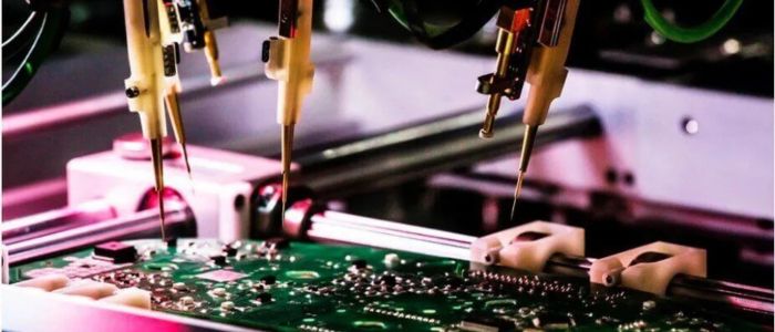
When a PCB fails, it feels like watching all your hard work vanish in seconds. Spotting issues before production starts saves time, money, and a few gray hairs.
The best tools for PCB inspection and defect detection are AOI systems, flying probe testers, X-ray machines, and microscopes. These help find soldering problems, misplaced parts, and even hidden internal faults early on.

Inspection tools might look fancy, but each one has a story. They tell how quality doesn’t start at the end of production, but right at the beginning. Without them, even the best design can go wrong. Let’s go deeper into these tools and see why each one truly matters.
What makes AOI (Automated Optical Inspection) a must-have in PCB manufacturing?
When you see a PCB line running fast, it’s easy to miss what’s really wrong until it’s too late. AOI acts like your eyes but sharper, faster, and more patient.
AOI machines use cameras and smart software to automatically check for missing parts, solder bridges, or wrong polarity. They compare each board to a reference image and flag anything that doesn’t match.

Why AOI matters for high-speed, accurate inspection
I remember my first time seeing an AOI system. It was scanning boards faster than I could blink. I thought it would miss something for sure. But no, it caught even the tiniest solder blob out of place.
Here’s what makes AOI tick and why manufacturers swear by it:
| AOI Feature | Description | Impact on Quality |
|---|---|---|
| High-speed cameras | Capture clear images from multiple angles | Catches tiny solder and placement errors |
| Image comparison | Checks each board against the golden sample | Makes sure every board looks right |
| Lighting control | Uses angled lights | Helps show micro-defects the eye can’t see |
| Error classification | Labels critical vs minor defects | Cuts down false alarms |
AOI works both before and after reflow. Before reflow, it finds misplaced parts. After reflow, it spots bad solder joints. It’s one of those machines that pays for itself fast, especially when the line runs 24/7.
Why are X-ray inspection systems vital for multilayer PCB defect detection?
Some defects hide too deep for cameras or eyes to see. They sit quietly inside layers, waiting to cause trouble later. That’s where X-ray inspection becomes the hero.
X-ray inspection exposes hidden problems like voids, cracks, or weak solder joints inside components such as BGAs and QFNs.

Seeing the unseen with X-ray precision
I once saw a board that passed all visual checks. It looked perfect. But it failed when powered up. We ran an X-ray scan and there it was — tiny air bubbles inside solder balls. Invisible outside, but deadly inside.
Here’s how X-ray tools help uncover those mysteries:
| Inspection Type | What It Detects | When It’s Used |
|---|---|---|
| 2D X-ray | Voids, bridges, missing solder | Fast surface-level checks |
| 3D CT X-ray | Internal cracks, buried vias | Deep structure inspection |
| Micro-focus X-ray | Fine cracks, slight misalignment | Precision-level testing |
For complex multilayer boards, X-ray inspection is like having X-ray vision. It tells you exactly what’s happening inside those hidden solder joints and buried traces.
What is the role of Flying Probe Testers in PCB defect detection?
Sometimes you don’t need speed, you need flexibility. That’s when flying probe testers come in. They’re perfect for prototypes and small batch runs.
Flying probe testers use moving needles to test connections, shorts, and component placement without needing a custom test fixture.

Why flexibility matters during prototype stages
I saw a small workshop using flying probe testing for their prototypes. They didn’t have to build any jigs or fixtures. They just loaded the program and started testing. That freedom saved them time and a lot of money.
Here’s how they make life easier:
| Feature | Purpose | Benefit |
|---|---|---|
| Auto probe movement | Moves between test points | Tests various designs easily |
| Continuity testing | Finds open and short circuits | Keeps circuits clean and stable |
| Component value check | Measures R and C values | Spots wrong or damaged parts |
| No fixture setup | No jigs required | Great for short runs and prototypes |
Flying probe testers might be slower than in-circuit testers, but their flexibility makes them a favorite for early design testing and low-volume production.
How effective is manual inspection under microscopes for visual defect detection?
Even with all the automation, sometimes nothing beats a pair of trained eyes. Manual inspection still has its place in PCB quality control.
Microscope inspection helps spot surface-level issues like solder cracks, lifted pads, or contamination that even smart machines can miss.

The human eye still plays a role
Once, I watched a technician inspecting boards through a stereo microscope. He suddenly pointed out a hairline crack near a connector pin that no machine had caught. It was so fine you’d miss it if you blinked. That’s when I realized why manual checks still matter.
Here’s how it stacks up with other methods:
| Inspection Method | Best For | Limitations |
|---|---|---|
| Manual microscope | Fine cracks, solder issues | Slower, depends on skill |
| AOI system | Fast visual scans | Can miss deep or odd defects |
| X-ray system | Hidden structural faults | High cost |
| Flying probe | Electrical tests | Slower for mass output |
Manual inspection gives that last layer of assurance. Machines are great, but skilled people catch what algorithms sometimes overlook.
Can in-circuit testing (ICT) improve overall PCB reliability?
A board might look good and still fail electrically. That’s why in-circuit testing is essential.
In-circuit testing checks how components behave when powered, confirming if everything is connected and working correctly.

Electrical truth over visual perfection
I like to think of ICT as a truth serum for circuits. Boards that look flawless sometimes tell a different story under ICT. Faulty resistors, wrong values, and solder shorts don’t hide from this test.
Here’s what ICT actually does:
| Test Category | What It Does | Common Findings |
|---|---|---|
| Continuity test | Checks all traces | Finds open lines |
| Value verification | Measures resistance or capacitance | Detects wrong components |
| Functional test | Simulates working conditions | Ensures logic circuits behave |
| Boundary scan | Uses JTAG | Finds hidden interconnect faults |
ICT gives valuable feedback to both design and assembly teams. Once set up, it delivers consistent, fast testing for thousands of boards.
How do thermal imaging tools detect hidden PCB issues?
Sometimes heat tells the truth better than any signal. Hotspots can reveal where failure starts before it becomes visible.
Thermal cameras detect unusual heat patterns across the PCB, helping spot shorts, high resistance points, or overheating components.

When temperature becomes a clue
One time we were testing a power board that kept failing. Everything seemed fine until we used a thermal camera. One small chip glowed brighter than the rest. Turned out, a cracked solder joint was to blame.
Here’s how thermal imaging helps you catch these early signs:
| Mode | Purpose | Result |
|---|---|---|
| Passive scan | Monitors normal heat flow | Finds hot components |
| Active scan | Applies controlled load | Exposes weak solder points |
| Infrared map | Displays temperature zones | Shows heat imbalance clearly |
Thermal imaging is fast, non-contact, and visual. It’s often the final test before shipment to make sure nothing overheats later.
Why combine multiple inspection tools for the best results?
No single tool tells the whole story. Each sees the PCB from a different angle. Using them together is what makes real quality control.
Combining AOI, X-ray, flying probe, and ICT ensures complete coverage, cutting down on returns and improving reliability.

The strength is in integration
Each stage matters. AOI checks the look. X-ray confirms the inside. ICT tests how it runs. Thermal imaging checks how it behaves under stress. Together, they form a full safety net.
| Tool | Focus Area | Inspection Level |
|---|---|---|
| AOI | Visual quality | Surface |
| X-ray | Hidden defects | Internal |
| Flying Probe | Electrical health | Prototype |
| ICT | Functional check | Production |
| Thermal Imaging | Heat patterns | Final test |
In PCB production, real quality is about connecting all these checks together. It’s not just finding what’s wrong — it’s making sure nothing slips through.
Conclusion
The right inspection tools turn risk into confidence. When AOI, X-ray, ICT, and thermal systems work together, every board leaves the line with reliability built in.